Field Emission Scanning Electron Microscopy
Schedule a MeetingField Emission Scanning Electron MicroscopyFE-SEM Testing
At Nishka Research, our Field Emission Scanning Electron Microscopy (FE-SEM) services offer unparalleled high-resolution imaging and surface analysis, essential for optimizing performance, quality and innovation across industries including pharmaceuticals, chemicals, materials science, engineering, electronics and more. FE-SEM allows us to observe surface morphology meticulously, providing critical insights into material structures at the nanometer scale.
What is FE-SEM?
FE-SEM uses a finely focused electron beam to scan the surface of samples, capturing ultra-high-resolution images. This technique is vital for detailed examination of surface topography, particle size and structural composition, making it indispensable in a wide range of industrial and scientific applications.
Key Advantages of FE-SEM
- Ultra-High Resolution: FE-SEM offers high magnifications up to 800,000X, revealing even the smallest surface features that influence material behavior.
- Surface Sensitivity: Accurately captures surface roughness, texture and irregularities, providing insights into how materials perform under stress, wear, or environmental exposure.
- Non-Destructive: FE-SEM imaging preserves the integrity of the sample, allowing for repeat analysis or further testing as it is non destructive technique.
- Versatile Applications: From pharmaceutical to electronic and engineering components, FE-SEM is adaptable across various materials and industries.
Industries Served
- Aerospace
- Automotive
- Biomedical/biotechnology
- Compound Semiconductor
- Data Storage
- Defense
- Displays
- Electronics
- Industrial Products
- Lighting
- Pharmaceutical
- Photonics
- Polymer
- Semiconductor
- Solar Photovoltaics
- Telecommunications
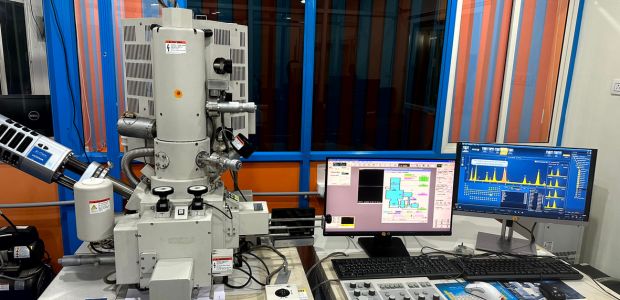
FE-SEM Instrument Details
- Make – HITACHI
- Instrument – Field Emission Scanning Electron Microscope (FE-SEM)
- Model – S-4800
- Magnification Range – Upto 8,00,000X
- Country of origin – JAPAN
Applications of FE-SEM across Industries
Pharmaceuticals:
- API Morphology and Particle Analysis: FE-SEM provides detailed high resolution images of Active Pharmaceutical Ingredients (APIs), showing particle size, shape and surface properties crucial for drug development.
- Polymorph Identification: FE-SEM helps to identify different polymorphic forms of drugs based on their physical structure, which can impact solubility, stability and therapeutic action.
Chemicals and Materials Science:
- Surface Topography and Composition: FE-SEM is ideal for examining surface texture and irregularities in chemical compounds and materials, revealing insights into mechanical properties in applications like coatings and polymers.
- Particle Size Distribution: Essential for ensuring consistent product quality in powders, catalysts and raw materials within the chemical industry.
Electronics and Semiconductors:
- Nanostructure Analysis: FE-SEM is critical for inspecting the micro- and nanostructures of electronic components, helping manufacturers detect defects or inconsistencies in semiconductors.
- Failure Analysis: Provides detailed imaging of fractures and imperfections, aiding in diagnosing the causes of component failure.
Polymers and Coatings:
- Surface Morphology:Allows manufacturers to examine surface texture and ensure product consistency in polymers and coatings, maintaining adherence to quality standards.
- Wear and Degradation Studies: Tracks surface changes due to environmental exposure, wear and chemical interactions, offering insights into product durability.
Automotive and Aerospace:
- Material Integrity: FE-SEM analyzes the surface characteristics of metals, alloys and composites, providing insights into material performance under stress, aiding in improving wear resistance.
- Failure Mode Analysis: Helps identify surface fractures, corrosionand fatigue in automotive and aerospace components, contributing to enhanced durability and safety.
Why ChooseNishka Research
- Accurate and Detailed Surface Analysis: Our FE-SEM systems deliver high-resolution images crucial for R&D and quality assurance across various industries.
- Customized Services: We tailor our FE-SEM analysis to your specific needs, ensuring that we address your unique industry challenges.
- Experienced Team: Our scientists and engineers expertly interpret complex FE-SEM data, delivering actionable insights that help improve product design and performance.
Regulatory Support across Industries
Our FE-SEM services come with comprehensive documentation and detailed analysis, supporting regulatory compliance and quality standards in industries such as pharmaceuticals, chemicals, electronics and materials science. Our reports meet the necessary requirements for product development, compliance and market entry.
Partner with Nishka Research for FE-SEM Services
Whether you’re working on new pharmaceutical formulations, investigating material integrity or optimizing electronic components, our FE-SEM services offer the precision and insights you need. Contact us today to discover how FE-SEM at Nishka Research can enhance your product development and quality control processes.
Looking for a trusted partner to achieve your research goals? schedule a meeting with us, send us a request, or call us at +91 78427 98518 to learn more about our services and how we can support you.
Need help or have a question?

Nishka Research Brochure
We deliver next-gen research services, Testing & Consultation know more..