Web Analytics

Scanning Electron Microscopy

Scanning Electron Microscopy / SEM Testing Lab

“Scanning electron microscopy (SEM) is a game-changing technique for the morphological, texture, failure analysis and microstructural composition analysis and the analysis of contaminants present in samples.”

Scanning Electron Microscopy is a test process that produces a magnified image of a sample using an electron beam for analysis. It is highly effective in micro-analysis and failure mode analysis of materials and composites.

SEM analysis can facilitate the analysis of microscopic and nanoscopic materials and objects with great precision. scanning electron microscopy technique. There are two methods of electron detection when using SEM. Backscattered electrons can help with the analysis of the elemental composition of the sample and the secondary electrons emitted close to the surface can reveal relevant information about the topography and morphology of the sample’s surface.  Combined with EDX, it can facilitate better analysis of the chemical and elemental composition of the samples.
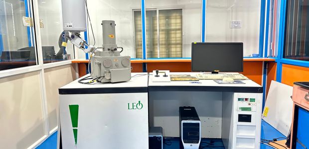
SEM Testing Lab in Hyderabad
Our operation of optical microscopes

At our labs and research centers, we make sure to use only the best equipment pieces so that no error can appear in the final results we will provide. Several precautions are maintained so that the sample under consideration does not get damaged during the study.

We ensure that during each new sample test, a sterile and disinfected slide is used for better results. Nishka professionals ensure that all the arrangement is perfect and no single object is out of the place so that the final data recorded can have the least flaws. The entire material is studied thoroughly with different samples belonging to the same category until the optima studies are obtained.

White Paper Download

Failure mode effects Investigation

Download

Risk and Failure analysis, Mitigation and Corrective services.

SEM Analysis Lab in Hyderabad
SEM Applications

SEM testing plays a critical role in the characterization of materials by producing a 2-D High-quality image of the sample. SEM can be used to analyze traits like external morphology, texture, topography and can be used to measure the thickness of the layered structures with the help of cross-sectional imaging. SEM, coupled with EDS, can reveal the chemical composition (Elemental Analysis) of a material. Particulate and contamination analysis gets accelerated by SEM coupled with Energy Dispersive X-ray spectroscopy (EDAX / EDS). It can facilitate and accelerate the investigation and study of interactions between substances and their substrates.

SEM testing is indispensable to mitigate contamination issues, perform failure mode and effects analysis and Identification & characterization of foreign particulates contamination. With the appropriate sampling methods, SEM becomes a powerful tool for an in-depth analysis.

Why Nishka?

NISHKA’s team of experts has vast experience with in-depth knowledge across various industries such as manufacturing, construction, power, chemicals, medicine and healthcare, electrical, electronics and polymers. This expertise can ensure Total Quality Assurance and can assist in mitigating issues, maintain regulatory standards, and study various materials with ease.

SEM analysis is critical for performing particle composition analysis. The high magnification imaging from our SEM analysis allows clients to understand the wear and tear properties of their material. Our SEM testing services provide analysis of the size, quantity and morphology of small particles. Using these analytical techniques, our team of experts can provide you with valuable insights to best optimize your product cycle.

Our Services
Energy Dispersive X-ray (EDX) Services
SEM/EDX allows analysis of elemental composition along with morphology and topography study of particles. The SEMs at NISHKA come equipped with EDX (also known as EDS). When exposed to an electron beam, the X-Rays emitted by an atom are unique, corresponding to its atomic number. EDX makes it possible to identify the elemental composition and sub-atomic properties of a sample. SEM analysis combined with EDX can help obtain more information and utilize analysis techniques appropriate for a given sample. EDX combined with SEM can be efficient to identify and examine samples at extremely high magnifications.
Remote View SEM Services

Remote View SEM facilitates a real-time interaction for a customer with the microscopist allowing direct failure mode analysis, surface feature analysis, particle morphology analysis, and chemical composition analysis to accelerate quality inspections or production speed. This mode enables a client to interact in real-time with a microscopist as they analyze a sample. Remote View SEM accelerates the failure mode analysis process and the production cycle highly. Remote-view SEM Imaging allows the client to execute better decision making with time efficiency and facilitates a better understanding of the features, morphology, and the elemental compositions of the samples by collaborating directly with the microscopist. This service is a game-changer in the failure analysis process.

Nishka routinely extends support for research, failure mode analysis, troubleshooting and quality control requirements to a multitude of clients across various industries, making us an ideal provider for your SEM analysis needs.

FAQs of Scanning Electron Microscope testing (SEM Analysis)

What is SEM analysis?

SEM analysis refers to the process of using a Scanning Electron Microscope (SEM) to examine the surface morphology of a sample at high magnification. The SEM uses an electron beam to scan the surface of the sample, producing high-resolution images that can reveal details about the sample's surface structure and by attaching EDAX we can be identify the composition.

What are the applications of SEM testing?

SEM testing is used in a variety of fields, including Pharmaceuticals, Materials science, Engineering, Biology and electronics. It is often used to study the surface morphology of materials, to identify the composition of substances, and to analyze the microstructure of materials.

How does SEM work?

In SEM testing, the sample is placed in a vacuum chamber and bombarded with a beam of electrons. These electrons will interact with the atoms in the sample, producing secondary electrons, backscattered electrons and X-rays. The secondary electrons are detected by the detector. These interactions provide information about the sample's structure and composition, which is used to create high-resolution 2D images of the sample.

What are the advantages of SEM?

SEM offers several advantages, including high magnification and resolution, the ability to observe both conductive and non-conductive materials (Sputter coated to make it conductive), and the ability to analyze a wide range of samples, from large objects to small particles.

What is sputter coating in SEM analysis?

Sputter coating is a process used in Scanning Electron Microscopy (SEM) to prepare non-conductive samples for analysis. The process involves depositing a thin layer of a conductive material, such as gold or platinum, onto the surface of the sample to make it conductive.

The sputter coating process works by bombarding the surface of the sample with a beam of positively charged particles, known as ions, which are emitted from a sputter source. The ions dislodge atoms from the surface of the sample, and the conductive material is deposited onto the sample to form a thin, uniform layer.

Sputter coating is important in SEM analysis because it enables the examination of non-conductive samples, which would otherwise not be visible in the SEM. By making the sample conductive, the electrons emitted by the SEM can interact with the sample and produce a high-resolution image.

It is important to note that sputter coating can alter the surface of the sample and introduce artefacts into the image. Therefore, it is important to choose a sputter coating material that is compatible with the sample and to carefully control the conditions of the sputter coating process to minimize the risk of sample damage and artefacts.

What are the limitations of SEM?

Here are few limitations of Scanning Electron Microscopy (SEM):

  1. Conductivity of sample: SEM requires that the sample being examined must be electro conductive or coated with a conductive material. This can limit the types of materials that can be analyzed using SEM.
  2. Vacuum essential: SEM operates in a vacuum environment, which can limit the types of samples that can be examined and the conditions under which they can be examined. Wet (Moistened) samples cannot be used in SEM.
  3. Sample preparation: SEM requires that samples be carefully prepared and mounted, which can be time-consuming and complex.
  4. Sample damage: There is a risk of sample damage during the SEM imaging process, especially for delicate or sensitive samples.
  5. Cost: SEM equipment and instrumentation can be expensive, and the process can be complex, requiring specialized knowledge and training.
  6. Resolution: While SEM provides high-resolution images, it may not be as sensitive as other imaging techniques, such as transmission electron microscopy (Even a nano particles can be examined), in terms of detecting subtle differences in sample structure and composition.

Nishka Research

NISHKA has been helping customers unlock their full potential and realize their true value for more than 13 years by providing innovative and bespoke solutions to ensure the highest standards.
View More

Nishka Research Pvt. Ltd.

Regus Business Center,
4th floor, Gumidelli Commercial Complex,
1-10-39 to 44, Old Airport Road, Begumpet,
Hyderabad-500016
India

Phone : +91 40 29303155

Mobile : +91 7842798518

Send Mail : [email protected]
Copyright © 2023 -NISHKA Research Pvt. Ltd. |
Privacy Policy
apartmentdatabasedownloadchevron-down
VENKATESH PANTHIKI
VENKATESH PANTHIKI

Left us a 5 star review

VENKATESH PANTHIKI
December 14, 2021
Narendar Vemula
December 14, 2021
Raviteja. Vathsavai
December 17, 2021
Samiksha More
June 2, 2022

Great work done by nishka research. Thank you so much for your kind Co operation

Keyur Butani
May 10, 2022

Submitted the samples for my phd work . Great work and reports submited with 2 days of time . Also the image clarity and all data are clear .

Divya Gaddam
December 15, 2021
Ramkumar Ganguly
April 25, 2022
Abhijit Patil
October 30, 2020

A very good lab delivering acurate results. I must also mention about the very cordial staff that they have.

sai charan
April 30, 2022
Ajay Gunti
December 14, 2021
akshay shriwas
December 14, 2021
M VENKAT M VENKAT
August 22, 2021
Chaithanya Reddy
December 30, 2021
Shyamala Mudiraj46
December 14, 2021
Tejaswini Kulakarni
December 14, 2021
Aishwarya Katrela
April 27, 2022
Andem Jhansi
December 14, 2021
Sai teja Reddy
March 1, 2022
KESHAMONI AKHILAGOUD
December 14, 2021
Firdose Begum
December 14, 2021
Anita Raj Panigrahi
October 20, 2021

Thank you for your services.. Looking forward for more collaboration with your labs for my future projects..

sushma nampally
December 15, 2021
Sashi Kanth
October 12, 2020

I am a PhD scholar from Kaunas University at Lithuania, Europe. I have given a sample to perform SEM analysis of the organic tissue. The results are highly satisfactory and impressive. The service was really excellent, on time( even before the time schedule), consumer friendly. cost to the academic samples are very less comparing with others. Once again thanks to Nishka for providing me the service ontime as I am really in urgency...

Yedukondalu Janapuram
December 14, 2021
linkedin facebook pinterest youtube rss twitter instagram facebook-blank rss-blank linkedin-blank pinterest youtube twitter instagram