Integrated Circuit (IC) devices are packaged in black boxes to protect the chip from the environment and to provide a standard outline for Printed Circuit Board (PCB) design and automatic pick and place. Chip, supporting leadframe and interconnection components are encapsulated inside the IC package. Epoxy molding compound is the most widely used material for IC encapsulation due to the low cost and good performance.
IC failure analysis may require looking into chips, wires, and devices that do not allow for observation of their internal parts because of their external package covering (Epoxy). The external layers blocking observation may be removed by proprietary techniques (chemical) etching to uncover the devices packaged inside for further treatment and observation during testing.

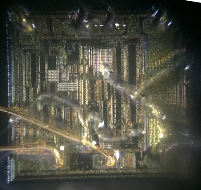
Decaping is the process of removing the black packaging material, which makes up a microchip in order to expose the silicon chip inside. The silicon chip inside is where all of the processing happens and is where the data is stored. In the case of a microcontroller, the kind you would find in most electronic devices, it is also where the firmware is stored.
In silicon chip, many secrets of integrated circuits are hidden, an analyst looking to uncover a failure. One has to extract silicon die and each layer has to be captured during the process to figure out failures. For microprocessors, there can be a different metal routing layers. Capturing of images can be done using normal optical microscopes to sophisticated instruments like SEM / TEM.
Applications :
Need help or Have a question?
Nishka Research Pvt. Ltd.
Regus Business Center,
4th floor, Gumidelli Commercial Complex,
1-10-39 to 44, Old Airport Road, Begumpet,
Hyderabad-500016
India
Phone : +91 40 29303155
Mobile : +91 7842798518
Left us a star review